Nature | Letter
Odd and even Kondo effects from emergent localization in quantum point contacts
- Journal name:
- Nature
- Volume:
- 501,
- Pages:
- 79–83
- Date published:
- DOI:
- doi:10.1038/nature12491
- Received
- Accepted
- Published online
A quantum point contact (QPC) is a basic nanometre-scale electronic device: a short and narrow transport channel between two electron reservoirs. In clean channels, electron transport is ballistic and the conductance is then quantized as a function of channel width1, 2 with plateaux at integer multiples of 2e2/h (where e is the electron charge and h is Planck’s constant). This can be understood in a picture where the electron states are propagating waves, without the need to account for electron–electron interactions. Quantized conductance could thus be the signature of ultimate control over nanoscale electron transport. However, even studies with the cleanest QPCs generically show significant anomalies in the quantized conductance traces, and there is consensus that these result from electron many-body effects3, 4. Despite extensive experimental and theoretical studies4, 5, 6, 7, 8, 9, 10, 11, understanding these anomalies is an open problem. Here we report that the many-body effects have their origin in one or more spontaneously localized states that emerge from Friedel oscillations in the electron charge density within the QPC channel. These localized states will have electron spins associated with them, and the Kondo effect—related to electron transport through such localized electron spins—contributes to the formation of the many-body state5, 6, 7. We present evidence for such localization, with Kondo effects of odd or even character, directly reflecting the parity of the number of localized states; the evidence is obtained from experiments with length-tunable QPCs that show a periodic modulation of the many-body properties with Kondo signatures that alternate between odd and even Kondo effects. Our results are of importance for assessing the role of QPCs in more complex hybrid devices12, 13 and for proposals for spintronic and quantum information applications14, 15. In addition, our results show that tunable QPCs offer a versatile platform for investigating many-body effects in nanoscale systems, with the ability to probe such physics at the level of a single site.
Subject terms:
At a glance
Figures
-
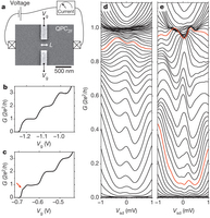
Figure 1: Conductance of quantum point contacts. a, Electron microscope image of a conventional quantum point contact (QPC) with two gate fingers (QPC2F). These gates are on the surface of a wafer with a 2DEG at 110 nm or 114 nm depth. Applying voltages Vg to these gates induces a narrow transport channel between source and drain regions of the 2DEG. The conductance of the QPCs is studied by applying and measuring voltage and current signals on contacts to the 2DEG. For QPC2F the length of the transport channel is fixed by the lithographic length L. b, c, Linear conductance G measured on two different QPC2F with L = 200 nm. The traces show clear quantized conductance plateaux at integer multiples of 2e2/h (the shift in dependence on Vg for c as compared to b is due to a different cool-down procedure; see Methods). The plateaux and transitions between plateaux show small deviations from clean quantized conductance behaviour, such as an additional shoulder at G ≈ 0.7(2e2/h) in c (red arrow). d, Nonlinear conductance G as a function of source–drain voltage Vsd at various Vg settings, for the device of b. The zero-bias anomaly (ZBA, enhanced conductance around Vsd = 0) has mostly single-peak character, but has double-peak character for G ≈ 0.9(2e2/h) (for example the red trace). e, Similar results as d for the device of c. In this device, ZBAs with double-peak character appear at G ≈ 0.1(2e2/h) and G ≈ 0.95(2e2/h).
-
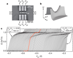
Figure 2: Length-tunable QPCs. a, Electron microscope image of a QPC with six gate fingers (QPC6F). It has a tunable effective length Leff that is set by operating at a fixed ratio Vg2/Vg1. b, Saddle-point potential that illustrates the electron potential energy U (without many-body interactions) in the 2DEG plane in a QPC region. c, Linear conductance G as a function of Vg1 (while co-sweeping Vg2 at fixed Vg2/Vg1) measured on a QPC6F for Leff tuned from 186 nm to 608 nm (traces are not offset). In addition to the quantized conductance plateau at 1(2e2/h), most traces show a smaller plateau in the range 0.7(2e2/h) to 0.9(2e2/h) due to many-body effects. For this signature of many-body effects, three periods of modulation can be observed in its dependence on Vg2/Vg1 (that is, Leff).
-
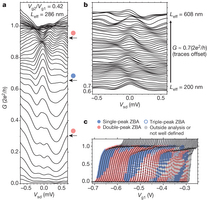
Figure 3: ZBAs in the nonlinear conductance of a QPC6F. a, Nonlinear conductance G as a function of source–drain voltage Vsd at various Vg1 settings, for operation at Leff = 286 nm. The ZBA appears alternately with single- or double-peak character. b, Evolution of the ZBA in the nonlinear conductance at fixed conductance level of ~0.7(2e2/h) as a function of Leff (traces offset). The ZBA has alternately single- or double-peak character. c, The character of the ZBA (single-, double- or triple-peak, as labelled) mapped out on the linear conductance data of Fig. 2c.
-
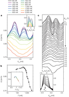
Figure 4: Comparison between experiments and theory of the Anderson model for a two-impurity Kondo system. a, Evolution of the nonlinear conductance (with double-peak ZBA) as a function of temperature for a QPC6F operated with fixed Vg1 = −0.528 V and fixed Vg2/Vg1 = 0.3 (traces not offset). Inset, calculated nonlinear-conductance traces from a two-impurity Kondo model (see main text). b, The conductance level of the traces in panel a near zero bias (between the two ZBA peaks, evaluated at Vsd = −0.02 mV) as a function of temperature (logarithmic axis). Inset, the same analysis applied to the theoretical results in the inset of a. c, Evolution of the nonlinear conductance (same device and operation point as a) as a function of applied in-plane magnetic field Bext (traces offset by −0.01(2e2/h)). Inset, calculated nonlinear-conductance traces from a two-impurity Kondo model.
Main
There are two signatures of many-body physics that are generically observed for a wide variety of QPCs, including systems in GaAs (refs 3, 9), Si (ref. 16) and graphene17, and that are found for transport of both electrons and holes9, 16. First, the quantized conductance traces often show the so-called 0.7 anomaly: an additional small plateau at about 0.7(2e2/h). Second, as a function of bias voltage across the channel, conductance G typically shows a peak around zero bias (named the zero-bias anomaly, ZBA), mostly below the first quantized plateau. The experimental observation5 that the ZBA and the 0.7 anomaly had similarities with the Kondo effect for quantum dots (transport through a single localized electron state18, 19) inspired theoretical work6, 7 that proposed that electron many-body physics could lead to localized electrons in the centre of the QPC. This is a remarkable phenomenon, because a QPC is a fully open quantum system. To avoid confusion with localization by an atomic impurity or disordered potential, these many-body states are termed self-consistent or emergent localized states (ELSs).
This theoretical work6, 7 developed the picture that the many-body effects in QPC channels are intimately related to the occurrence of a Friedel oscillation—an oscillation in the electron charge density that occurs when electron waves get reflected in a partially open QPC channel—which gets enhanced into an ELS with the charge of about one electron owing to Coulomb repulsion and exchange interactions between electrons. This reduces the conductance and can explain the 0.7 anomaly6. However, transport through such a state can be enhanced by the Kondo effect at temperatures below a typical Kondo temperature, TK. This appears as a ZBA and also moves the 0.7 plateau towards unity (in units of 2e2/h), consistent with experiments. This theoretical work6, 7 also predicted that, depending on parameters, a pair of such ELSs may emerge in the channel, resulting in a double-peak ZBA (as observed in double quantum dots20 owing to the two-impurity Kondo effect21, 22, 23, 24, 25, 26). So far no such double-peak ZBAs have been reported for QPCs (Supplementary Information section 3).
We report here the observation of such double-peak ZBAs in a large number of conventional QPCs (with two gate fingers as in Fig. 1a, denoted QPC2F). We also introduce a new type of QPC which has a tunable channel length (with six gate fingers as in Fig. 2a, denoted QPC6F). In these devices, the 0.7 anomaly and the ZBA show a periodic modulation as a function of QPC length, which we attribute to an increasing number of ELSs. Thus, as the number of ELSs increases with QPC length, its parity alternates, giving rise to modulation between Kondo effects for an odd or even number of localized states (known as odd- and even-impurity Kondo effects), and, as a result, between single- and double-peak ZBAs. In addition, the 0.7 anomaly shows a periodic modulation because the enhancement of the 0.7 feature towards unit conductance depends on both the parity and the parameters of the Kondo system such as TK, and these are both modulated as a function of QPC length.
.jpg)
a, Electron microscope image of a conventional quantum point contact (QPC) with two gate fingers (QPC2F). These gates are on the surface of a wafer with a 2DEG at 110 nm or 114 nm depth. Applying voltages Vg to these gates induces a narrow transport channel between source and drain regions of the 2DEG. The conductance of the QPCs is studied by applying and measuring voltage and current signals on contacts to the 2DEG. For QPC2F the length of the transport channel is fixed by the lithographic length L. b, c, Linear conductance G measured on two different QPC2F with L = 200 nm. The traces show clear quantized conductance plateaux at integer multiples of 2e2/h (the shift in dependence on Vg for c as compared to b is due to a different cool-down procedure; see Methods). The plateaux and transitions between plateaux show small deviations from clean quantized conductance behaviour, such as an additional shoulder at G ≈ 0.7(2e2/h) in c (red arrow). d, Nonlinear conductance G as a function of source–drain voltage Vsd at various Vg settings, for the device of b. The zero-bias anomaly (ZBA, enhanced conductance around Vsd = 0) has mostly single-peak character, but has double-peak character for G ≈ 0.9(2e2/h) (for example the red trace). e, Similar results as d for the device of c. In this device, ZBAs with double-peak character appear at G ≈ 0.1(2e2/h) and G ≈ 0.95(2e2/h).
.jpg)
a, Electron microscope image of a QPC with six gate fingers (QPC6F). It has a tunable effective length Leff that is set by operating at a fixed ratio Vg2/Vg1. b, Saddle-point potential that illustrates the electron potential energy U (without many-body interactions) in the 2DEG plane in a QPC region. c, Linear conductance G as a function of Vg1 (while co-sweeping Vg2 at fixed Vg2/Vg1) measured on a QPC6F for Leff tuned from 186 nm to 608 nm (traces are not offset). In addition to the quantized conductance plateau at 1(2e2/h), most traces show a smaller plateau in the range 0.7(2e2/h) to 0.9(2e2/h) due to many-body effects. For this signature of many-body effects, three periods of modulation can be observed in its dependence on Vg2/Vg1 (that is, Leff).
The signatures of a pair of ELSs are more likely to be observed on shorter QPCs7. We thus focused on QPC2F of lithographic length L = 200 nm (and width W = 350 nm), which is shorter than most QPCs reported in the literature. We searched for double-peak ZBAs in a set of 80 QPC2F (realized in two different wafer materials, different fabrication runs, different cool-downs, and with or without gate-biased cool-down; see Methods) and found them in about half the studied devices. The ubiquity of the phenomenon, and the fact that such double-peak ZBAs were persistently observed in the same devices over different cool-downs, implies that it is a generic effect and not due to a fortuitous impurity nearby. Figure 1 presents data from two QPC2F to illustrate that the signatures of many-body physics show qualitatively similar features, though with significant device-to-device variation (whereas there is no strong variation in the manifestation of non-interacting electron physics, such as the quantized conductance8, 10). Figure 1b, c presents measurements of the linear conductance (Methods). In addition to the quantized conductance plateaux at integer multiples of 2e2/h, the trace in Fig. 1c shows an additional shoulder at G ≈ 0.7(2e2/h) (the 0.7 anomaly, also observed for the device of Fig. 1b at higher temperatures). Results for the nonlinear conductance (Methods) of these same devices are presented in Fig. 1d, e. Most traces between 0 and 1(2e2/h) show a single-peak ZBA (the enhancement of conductance within ±0.5 mV around Vsd = 0 mV, where Vsd is the bias voltage across the channel). However, the red traces mark examples where the ZBA appears with double-peak character (the asymmetric character of these nonlinear conductance traces will be discussed below). For double-peak ZBAs just below 1(2e2/h), we typically observe a peak splitting that increases with conductance.
Theoretical work7 predicted that the Friedel oscillation resulting from the screening of the QPC potential would create two electron ‘puddles’, one on each side of the QPC. For most QPC geometries, it showed that lowering the potential by means of the gate voltage would give a single ELS in the centre of the QPC because the Friedel oscillations from both sides connect. However, for short QPCs (for L similar to the Fermi wavelength) the two ELSs remain intact as the potential is lowered. This gives the physics of a two-impurity Kondo system, and as the coupling between them gets stronger with increasing conductance, the ZBA splits22, 23, 24, 25, 26. At lower conductance values, the ZBA may appear as a single or a double peak, depending on the ratio between the Kondo temperature of the two ELSs and the strength of interaction between them. Although this is fully consistent with our observations (Fig. 1d, e), the coupling between these ELSs and the resulting splitting of the ZBA depend very sensitively on the device dimensions and the always-present remote imperfections (Supplementary Information section 4), and this leads to significant variability among devices. Thus, a more stringent test of this picture is possible with QPCs whose parameters can be modified continuously.
We addressed this by investigating a set of eight QPC6F devices, for which we could gradually change the effective length Leff of the saddle-point potential. These devices showed qualitatively identical behaviour, with an oscillatory signature of the 0.7 anomaly and regular modulation between single- and double-peak ZBAs with increasing Leff (Fig. 3b, c). These reproducible observations on eight QPC6F (and for different cool-downs of one QPC6F; Supplementary Information section 10) are consistent with the emergence of an increasing number of ELSs due to many-body physics that generically occurs, even in ultra-clean QPC channels.
.jpg)
a, Nonlinear conductance G as a function of source–drain voltage Vsd at various Vg1 settings, for operation at Leff = 286 nm. The ZBA appears alternately with single- or double-peak character. b, Evolution of the ZBA in the nonlinear conductance at fixed conductance level of ~0.7(2e2/h) as a function of Leff (traces offset). The ZBA has alternately single- or double-peak character. c, The character of the ZBA (single-, double- or triple-peak, as labelled) mapped out on the linear conductance data of Fig. 2c.
Figure 2a depicts the QPC6F devices, for which the effective channel length Leff could be tuned continuously. These were operated with the central gate voltage Vg1 more negative than the side gate voltage Vg2, to avoid quantum dot formation. Our analysis shows that in this regime the gates induce a smooth saddle-point potential, despite the narrow gaps between the gate fingers. The effective channel length Leff is set by Vg2/Vg1 (short for Vg2/Vg1 near 0, long for Vg2/Vg1 near 1; see Supplementary Information section 5 for details). Our devices could thus be controlled to have Leff in a range from about 186 nm to 608 nm. Making Vg1 less negative, at a fixed ratio Vg2/Vg1, opens the QPC while keeping the length unchanged.
All QPC6F showed clear quantized conductance plateaux. Figure 2c shows for one device how the 0.7 anomaly appears as an additional plateau (smaller than the quantized conductance plateaux) in the range 0.7(2e2/h) to 0.9(2e2/h), and that this plateau shows a dependence on Leff, with three periods of modulation for the range Leff = 186 nm to 608 nm. The nonlinear conductance measurements from this device (Fig. 3a) show how the ZBAs appear for Leff = 286 nm. At a fixed length, the ZBAs alternate between single-peak and double-peak character when opening the QPC, again with increased splitting for the double-peak ZBA as the conductance approaches 1(2e2/h). The overall appearance of the ZBAs is very similar to that of fixed-length QPC2F (Fig. 1d, e). Figure 3b shows that there is also a modulation between single- and double-peak character when increasing Leff at a fixed conductance level (as evaluated immediately next to the ZBA). Figure 3c plots the data of Fig. 2c again, with coloured data symbols on the traces that mark whether the ZBA at that point has single- or double-peak character (in some cases, we find ZBAs that are best described as triple-peak). The modulation between single-peak and double-peak ZBA as a function of Leff also shows about three periods, and is clearly correlated with the modulation of the 0.7 anomaly.
To critically check the relevance of two-impurity Kondo physics to our observations, we measured the temperature and magnetic field dependence of double-peak ZBAs and compared these with theory for this system. We obtained the theoretical results by calculating the current through a two-impurity Anderson model. For this model, one expects22, 23, 24, 25, 26 a current that gets enhanced by the Kondo effect when the temperature is lowered from above the Kondo temperature to below it. Depending on the strength of the effective coupling between the impurities relative to the Kondo temperature, the associated ZBA has either single- or double-peak character.
Figure 4a depicts how the nonlinear conductance develops from a background conductance of 0.75(2e2/h) at 3,000 mK into a double-peak ZBA with peak values up to about 0.90(2e2/h) as the temperature is decreased (we used the device of Fig. 3; Supplementary Fig. 9 shows the temperature dependence of the linear conductance). The conductance between the peaks (the linear conductance) has a non-monotonic temperature dependence (Fig. 4b) that is characteristic of two-impurity Anderson physics27. For comparison, insets in Fig. 4a and b depict the results of the theoretical calculations, and show good qualitative agreement. (We note that this description calculates only the Kondo contribution to the current, which yields zero current at high temperatures owing to Coulomb blockade; in contrast, the ELSs in QPCs are not expected to show strong Coulomb blockade at high temperatures but rather a finite background conductance, as observed.) The theoretical traces are calculated for two impurity sites with unequal coupling strength Γ to a neighbouring electron reservoir, and accordingly an unequal Kondo temperature TK (the plots are presented on an energy scale given by the highest Kondo temperature of the two sites). The asymmetry between the two Γ parameters gives asymmetric double-peak ZBAs, with the minimum conductance between the peaks not exactly at Vsd = 0, very similar to the experimentally observed double-peak ZBAs. We should expect such asymmetries between the two Γ parameters, because the Γ values depend exponentially on the coupling between the ELSs and the electron reservoirs (Supplementary Information section 4).
.jpg)
a, Evolution of the nonlinear conductance (with double-peak ZBA) as a function of temperature for a QPC6F operated with fixed Vg1 = −0.528 V and fixed Vg2/Vg1 = 0.3 (traces not offset). Inset, calculated nonlinear-conductance traces from a two-impurity Kondo model (see main text). b, The conductance level of the traces in panel a near zero bias (between the two ZBA peaks, evaluated at Vsd = −0.02 mV) as a function of temperature (logarithmic axis). Inset, the same analysis applied to the theoretical results in the inset of a. c, Evolution of the nonlinear conductance (same device and operation point as a) as a function of applied in-plane magnetic field Bext (traces offset by −0.01(2e2/h)). Inset, calculated nonlinear-conductance traces from a two-impurity Kondo model.
Figure 4c presents the measured magnetic field dependence of this double-peak ZBA. Theoretically, one expects different evolutions with magnetic field depending on the relative magnitude of parameters—such as the Kondo temperature of each impurity, the coupling between the impurities, the asymmetry between the impurities and the temperature. The possibilities include each peak splitting into two sub-peaks, the peaks getting closer and merging, and the peaks moving closer and crossing each other. We see such diverse dependence on magnetic field for the different operation points of a given device, and for different devices. Figure 4c shows one example, with a comparison to the theoretical expectations (other examples are given in Supplementary Information section 8). We see again good qualitative agreement between the theory of the two-impurity model and the experimental observations.
From the width of the peaks in Fig. 4a we can estimate the Kondo temperature TK, and the splitting between the peaks is equal to twice the effective coupling between the two ELSs. This coupling is here ~0.2 meV (a typical value for the larger data set plotted in Fig. 3c). This should be consistent with the temperature at which the double-peak character of the ZBA is no longer resolved (and the temperature where the non-monotonic temperature dependence of conductance has a maximum27). In Fig. 4a, this occurs for ~800 mK (that is, ~0.1 meV). This is in reasonable agreement with the distance between the peaks. The fact that it is on the low side is probably because TK is here at the same energy scale as the splitting (~0.15 meV when estimated as half the peak widths in Fig. 4a). We also analysed ZBAs with pronounced single-peak character in the same manner as in ref. 5, and found agreement with the single-impurity Kondo model to the same extent.
The increase of Leff that induces one period of modulation for the 0.7 anomaly and the split-peak character of the ZBA in Fig. 3 (~100 nm to ~150 nm) matches the Fermi wavelength in the QPC channel (Supplementary Information section 6). This supports the hypothesis that the periodicity is linked to Friedel oscillations in the channel which gradually develop additional periods as it gets longer. (That such Friedel oscillations occur on scattering in a two-dimensional electron gas, 2DEG, has been observed directly in a different setting28.) The increasing number of ELSs with channel length leads to alternation between odd- and even-impurity Kondo effects, and to modulation between single-peak and double-peak ZBAs, respectively (the three-impurity case was studied in ref. 29 and can show ZBAs with triple- or predominantly single-peak character).
To support this picture, we carried out numerical spin density functional theory (SDFT) calculations, generalizing earlier work7 (Supplementary Information section 2). The length of the channel was determined by a gate of variable length. We studied whether SDFT yields localized states with the charge of about one electron as the state with lowest energy. The results (an example is in Supplementary Fig. 1) show an increasing number of ELSs as the channel gets longer, and also as the QPC is opened by lowering the QPC saddle-point potential at fixed length. These calculations support the picture we have presented here: the number of ELSs increases by one each time the QPC length increases over a range that allows for one additional period of the Friedel oscillation in the QPC channel. The SDFT results suggest that, depending on the overlap of the ELSs, higher spin states (S = 1 or S = 3/2) may develop in the QPC, making it possible to study Kondo effects for higher spin, and enabling investigation of transport through such exotic states.
The emergence of a ZBA for a hybrid device with a semiconductor channel was recently reported as a signature of Majorana fermions12. The fact that similar ZBAs occur with rich behaviour in plain semiconductor QPCs suggests that one should be cautious when ruling out alternative explanations for these Majorana signatures13. Evidently, basic understanding of the physics in QPCs is a crucial step in understanding more complex hybrid structures. Tunable QPCs offer an excellent new test ground for such studies, and they are also suited for detailed studies of Friedel oscillations30 and strongly correlated electrons in low dimensions, at the level of a single site.